Preparation and growth mechanism of ultra-thin free-standing polycrystalline diamond film based on glass carbon substrate
-
摘要:
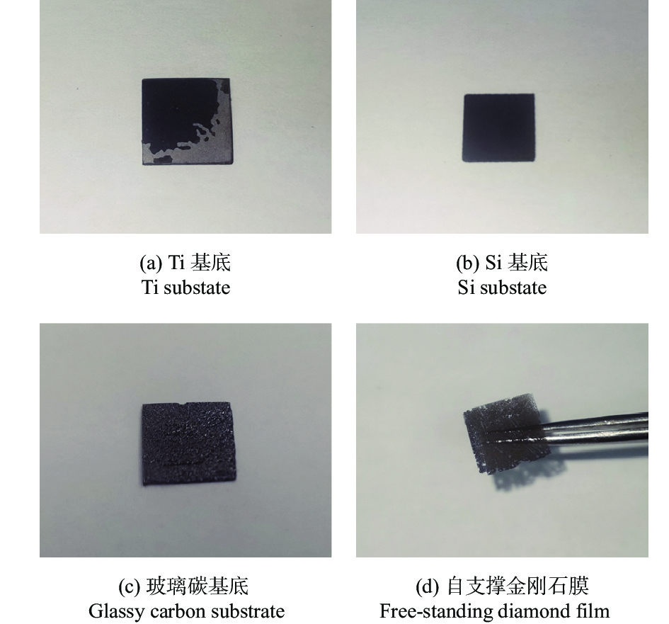
选取Ti、Si、玻璃碳3种基底,采用微波等离子体化学气相沉积技术,以CH4/H2为反应源制备超薄多晶金刚石膜。通过SEM、Raman、台阶仪表征并分析所制备的金刚石薄膜整体形态、表面(断面)形貌、组成、应力状态等。结果表明:仅以玻璃碳为基体生长的金刚石膜能自动剥离形成完整自支撑体,且薄膜表面晶粒的晶面显形清晰,膜厚仅为10 μm; Raman光谱表征表明薄膜呈强的尖锐金刚石特征峰,且计算的残余应力最低,仅有−0.2161 GPa。可为超薄自支撑CVD金刚石膜的一步法生长-剥离提供新的技术途径。
Abstract:[Objective] Diamond films have been widely used in many fields such as semiconductor devices, optical windows, biomedical applications, heat sink, and mechanical tooling. High quality diamond films need be completely peeled off from the substrate surface for subsequent processing. However, there are still significant challenges in achieving the complete detachment of films. In this paper, a free-standing ultra-thin diamond film with a thickness of about 10 μm and high purity was fabricated using the microwave plasma chemical vapor deposition (MPCVD) method on a glass carbon substrate.
[Method] Three types of substrates, namely titanium (Ti), silicon (Si) and glass carbon, were selected for the fabrication of ultra-thin polycrystalline diamond films using MPCVD with a CH4-H2 mixture as the precursor. The pretreatment for nucleation involved mechanical polishing, followed by ultrasonic vibration-assisted machining with a suspension of diamond microns. The pre-treated substrates were thoroughly cleaned and placed in the MPCVD deposition chamber for growing diamond films under the following conditions: microwave power 5.4 kW, hydrogen (99.99999%) flow rate of 200 sccm, methane (99.99999%) flow rate of 10 sccm, substrate temperature of 870 ℃, chamber pressure of 17.5 kPa, and deposition time of 180 min. SEM, Raman spectrometer and surface profilometer were used to the characterize the overall morphology, surface and cross-sectional surface topography, phase composition, and stresses of the thin diamond films deposited on the three different substrates.
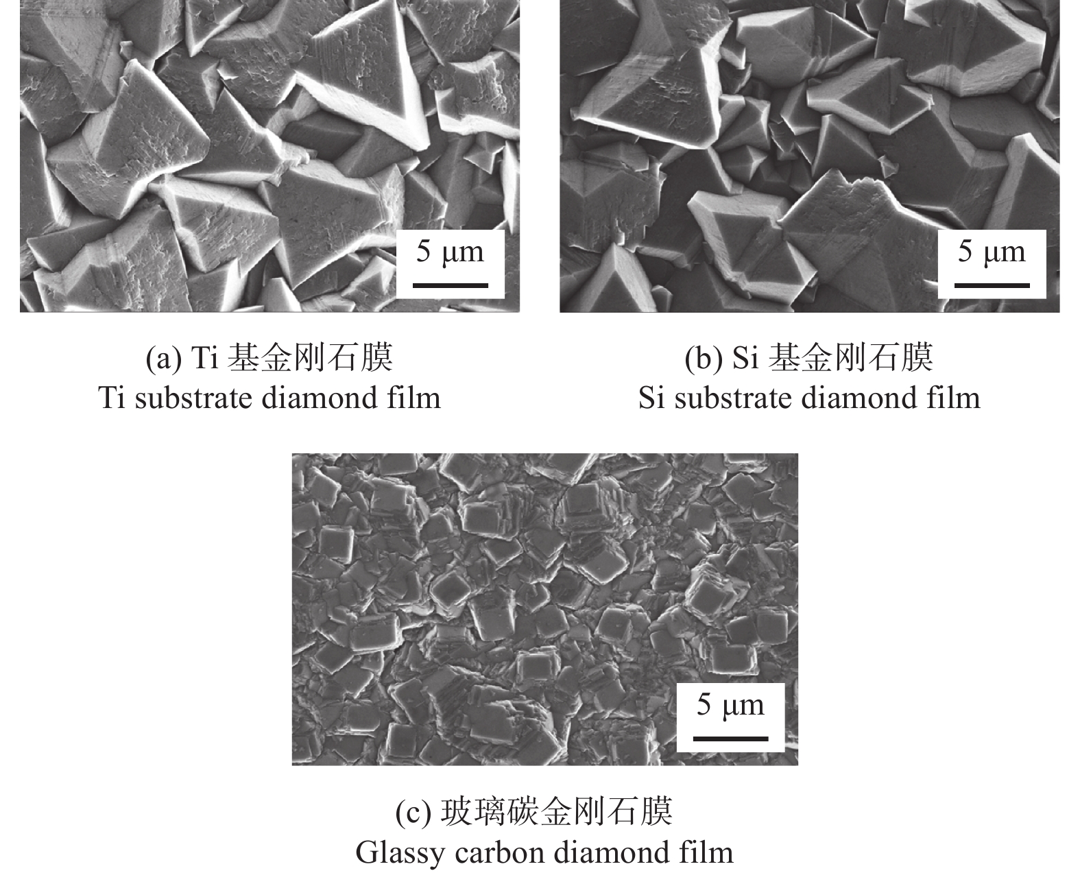
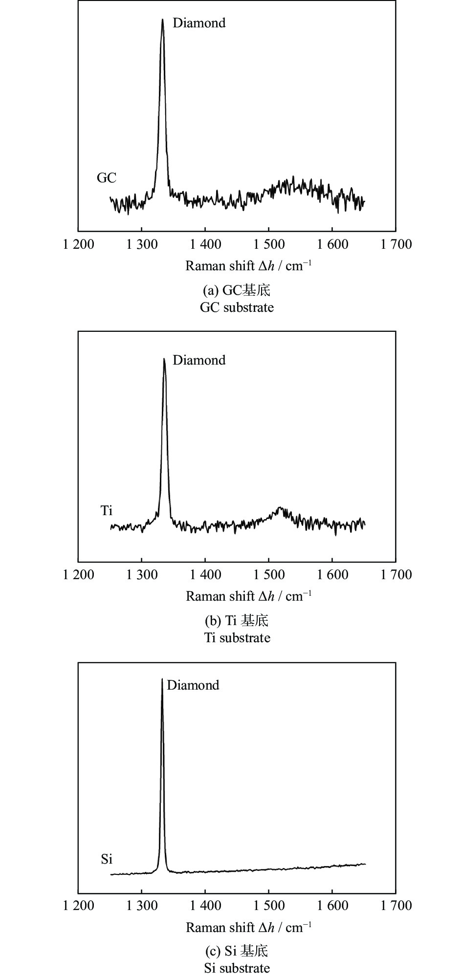
[Results] It was found that the ultra-thin free-standing diamond films grown on the glass carbon substrates were relatively intact with a smooth surface and minimal warping. SEM images revealed that the crystal shapes of all the three diamond films were distinct with tightly bonded grains. The surface topography of the films grown on Ti and Si substrates was similar, both with octahedral surface grains and (111) preferentially oriented crystal plane. In contrast, the grains of diamond films grown on glass carbon substrate (GCD) were mainly cubic, showing a preferential orientation along the (100) crystal plane. Raman spectra of diamond films on different substrates showed strong and sharp characteristic peaks of diamond, indicating high purity and complete crystal structures in all three films. Further analysis of the shift (Δh) between intrinsic peak and characterized Raman peaks revealed that the residual stress in GCD was minimal and predominantly compressive, effectively preventing the occurrence of cracks or fractures in the film and ensuring the integrity of the free-standing films. Conversely, Ti-based diamond films experienced the largest residual stress due to significant differences in their thermal expansion coefficients, which inevitably ld to larger thermal stresses between the diamond film and Ti substrate during cooling. Glassy carbon and diamond had similar thermal expansion coefficients, resulting in smaller thermal stresses during cooling, which was beneficial for the integrity of the free-standing film.
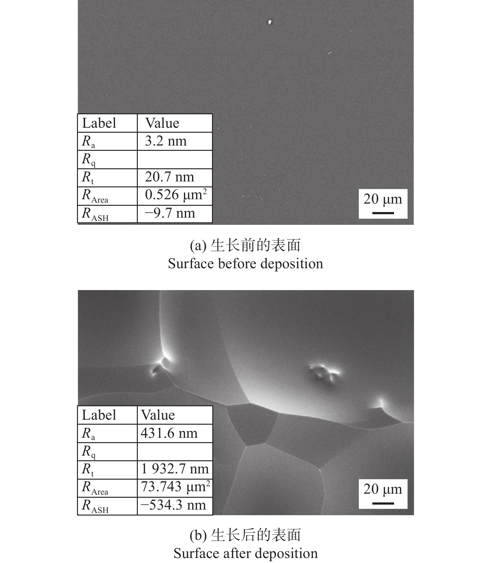
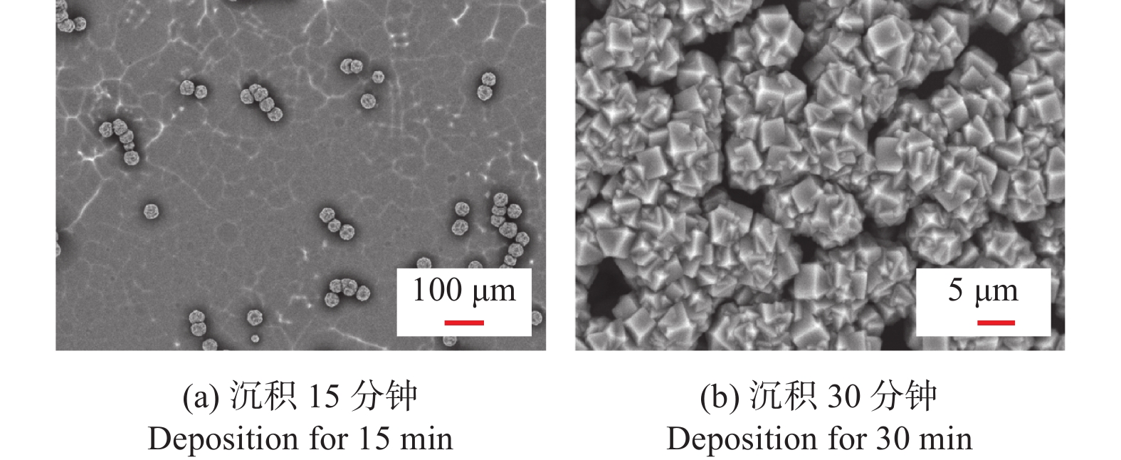
SEM images of the glassy carbon substrate surface before and after growth showed that the surface of the glassy carbon substrate was originally smooth and flat, with a surface roughness of Ra=3.2 nm as measured by a step profiler. Due to the etching effect of H plasma on non-diamond carbon, sand dune-like undulations appeared on the surface of the glassy carbon after the film growth, with a surface roughness of Ra=431.6 nm. This surface morphology weakened the interfacial bonding strength between the diamond film and the substrate, creating a gap between the film material and the substrate. Moreover, as the glassy carbon substrate continued to be etched during the deposition process and the gap widened, the bonding strength at the film-substrate interface would be further weakened. From the SEM images of the substrate surface at different depositing times in the early stages of growth, it was inferred that the process of growing free-standing diamond films on glassy carbon substrates proceeded as follows: during the nucleation stage, carbon-containing precursors formed island-like nuclei on the substrate surface, while the glassy carbon substrate surface was exposed to an H plasma atmosphere and etched into sand dunes. The island-like nuclei then grew into a complete diamond film through an island growth mode.
[Conclusion] Glassy carbon can be effectively used as a substrate to prepare ultra-thin, high-purity free-standing diamond films with a thickness of approximately 10 μm using the MPCVD method. The mechanism for achieving one-step growth and self-supporting peeling of the ultra-thin diamond film is mainly through the etching of the glassy carbon substrate by hydrogen plasma to weaken the interfacial bonding force, ultimately achieving self-peeling. At the same time, the low residual stress of the film material itself ensures the integrity of the film. Choosing glassy carbon as the substrate represents an effective technical approach for meeting the preparation requirements of ultra-thin free-standing diamond films.
-
Key words:
- ultra-thin diamond film /
- free-standing /
- glass carbon substrate /
- film-substrate separation /
- growth mechanism /
- MPCVD
-

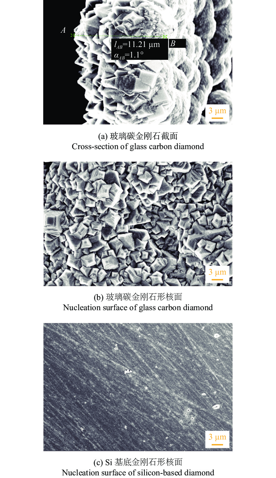
图 4 GCD膜的截面、形核面及Si基底金刚石形核面SEM图
Figure 4. SEM diagrams of cross-section and nucleation surface of GC substrate diamond film and nucleation surface of Si substrate diamond

图 5 生长前后玻璃碳基底的表面SEM图
Figure 5. Surface SEM of a glass-carbon substrate before and after growth

图 6 玻璃碳基底上不同沉积时间的SEM图
Figure 6. SEM plots of different nucleation times on glassy carbon substrate
表 1 不同基底CVD膜的性能参数
Table 1. Performance parameters of CVD membranes with different substrates
基底 峰位 h / cm−1 偏移量 Δh / cm−1 应力状态 残余应力 σ / GPa Ti 1335.6627 3.1627 压应力 −1.9523 Si 1331.7312 −0.7688 张应力 0.4746 GC 1332.8501 0.3501 压应力 −0.2161  下载: 导出CSV
-
[1] LAM S E, BRADLEY D A, KHANDAKER M U. Small-field radiotherapy photon beam output evaluation: Detectors reviewed [J]. Radiation Physics and Chemistry,2021,178:108950. doi: 10.1016/j.radphyschem.2020.108950 [2] GUTHRIE M, PRUTEANU C G, DONNELLY M-E, et al. Radiation attenuation by single-crystal diamond windows [J]. Journal of Applied Crystallography,2017,50(1):76-86. doi: 10.1107/S1600576716018185 [3] MARINELLI M, FELICI G, GALANTE F, et al. Design, realization, and characterization of a novel diamond detector prototype for FLASH radiotherapy dosimetry [J]. Medical Physics,2022,49(3):1902-1910. doi: 10.1002/mp.15473 [4] SATURDAY L, WILSON L, RETTERER S, et al. Thermal conductivity of nano- and micro-crystalline diamond films studied by photothermal excitation of cantilever structures [J]. Diamond and Related Materials,2021,113:108279. doi: 10.1016/j.diamond.2021.108279 [5] LUO S Y, HO J K, TSAI M Y, et al. A study of the diamond tools for grinding polycrystalline diamond [J]. Advanced Materials Research,2010,585:126-128. doi: 10.4028/www.scientific.net/AMR.126-128.585 [6] LIU L Y, OUYANG X P, ZHANG J F, et al. Properties comparison between nanosecond X-ray detectors of polycrystalline and single-crystal diamond [J]. Diamond and Related Materials,2016,73:248-252. doi: 10.1016/j.diamond.2016.10.002 [7] 李义锋. 新型高功率MPCVD装置研制与金刚石膜高效沉积 [D]. 北京: 北京科技大学, 2015.LI Yifeng. Design of high power MPCVD reactors and synthesis of high quality diamond films [D]. Beijing: University of Science and Technology Beijing, 2015. [8] YING X, LUO J, WANG P, et al. Ultra-thin freestanding diamond window for soft X-ray optics [J]. Diamond and Related Materials,2003,12:719-722. doi: 10.1016/S0925-9635(02)00340-0 [9] SHVYD’KO Y, BLANK V, TERENTYEV S. Diamond x-ray optics: Transparent, resilient, high-resolution, and wavefront preserving [J]. MRS Bulletin,2017,42(6):437-444. doi: 10.1557/mrs.2017.119 [10] DING M, LI L, DU Y, et al. Correlation between growth mechanism of microcrystalline diamond-ultrananocrystalline diamond composite and mechanical properties of its thin THz TWT windows: "Proceedings of IEEE International Vacuum Electronics Conference (IVEC)" [C/OL]. IEEE: Monterey, CA, USA, 2018: 249-250[2023-05-07]. https://ieeexplore.ieee.org/document/8391667 [11] HAQUE M S, NASSEM H A, MALSHE A P, et al. A study of stress in microwave plasma chemical vapor deposited diamond films using X-Ray diffraction [J]. Chemical Vapor Deposition,1997,3(3):129-135. doi: 10.1002/cvde.19970030304 [12] MOKUNO Y, CHAYAHARA A, YAMADA H. Synthesis of large single crystal diamond plates by high rate homoepitaxial growth using microwave plasma CVD and lift-off process [J]. Diamond & Related Materials,2007,17(4/5):415-418. doi: 10.1016/j.diamond.2007.12.058 [13] MOKUNO Y, KATO Y, TSUBOUCHI N, et al. A nitrogen doped low-dislocation density free-standing single crystal diamond plate fabricated by a lift-off process [J]. Applied Physics Letters,2014,104(25):252109. doi: 10.1063/1.4885552 [14] LIU Z, CHEN L, LI C, et al. Thermal stress in free-standing diamond films with Cr interlayer destroyed [J]. Journal of Materials Science and Technology,2010,26(11):991-995. doi: 10.1016/S1005-0302(10)60162-4 [15] GUO J, LIU J, HUA C, et al. Interfacial stress evolution simulation on the graphite substrate/interlayer/diamond film during the process [J]. Diamond and Related Materials,2017,75:12-17. doi: 10.1016/j.diamond.2016.12.017 [16] TERRANOVA M L, ROSSI M, SESSAL V, et al. Development of different carbon phases during diamond film growth by CVD on glassy carbon substrates [J]. Solid State Communications,1994,91(1):55-58. doi: 10.1016/0038-1098(94)90842-7 [17] SANKARAN K J, FICEK M, KUNUKU S, et al. Self-organized multi-layered graphene-boron-doped diamond hybrid nanowalls for high-performance electron emission devices [J]. Nanoscale,2018,10(3):1345-1355. doi: 10.1039/C7NR06774G [18] KAUR G, PULAGARA N V, KUMAR R, et al. Metal foam-carbon nanotube-reduced graphene oxide hierarchical structures for efficient field emission [J]. Diamond and Related Materials,2020,106:107847. doi: 10.1016/j.diamond.2020.107847 [19] VLASOV I, RALCHENKO V, ZAKHAROV D, et al. Intrinsic stress origin in high quality CVD diamond films [J]. Physica Status Solidi (A),1999,174(1):11-18. doi: 10.1002/(SICI)1521-396X(199907)174:1<11::AID-PSSA11>3.0.CO;2-T [20] MUKHOPADHYAY D. Identifying the causes of residual stress in polycrystalline diamond compact (PDC) cutters by X-Ray diffraction technique [J]. Results in Materials,2021,11(580):100216. doi: 10.1016/j.rinma.2021.100216 [21] HINZMANN D, BöTTCHER, REIMERS W, et al. Ex situ residual stress analysis of chemical vapor deposited diamond coated cutting tools by synchrotron X-Ray diffraction in transmission geometry [J]. Advanced Engineering Materials,2021,23(11):2001525. doi: 10.1002/adem.202001525 [22] GRACIO J J, FAN Q H, MADALENO J C. Diamond growth by chemical vapour deposition [J]. Journal of Physics D:Applied Physics,2010,43(37):374017. doi: 10.1088/0022-3727/43/37/374017 -

 点击查看大图
计量
- 文章访问数: 1168
- HTML全文浏览量: 476
- PDF下载量: 163
- 被引次数: 0
 邮件订阅
邮件订阅 RSS
RSS